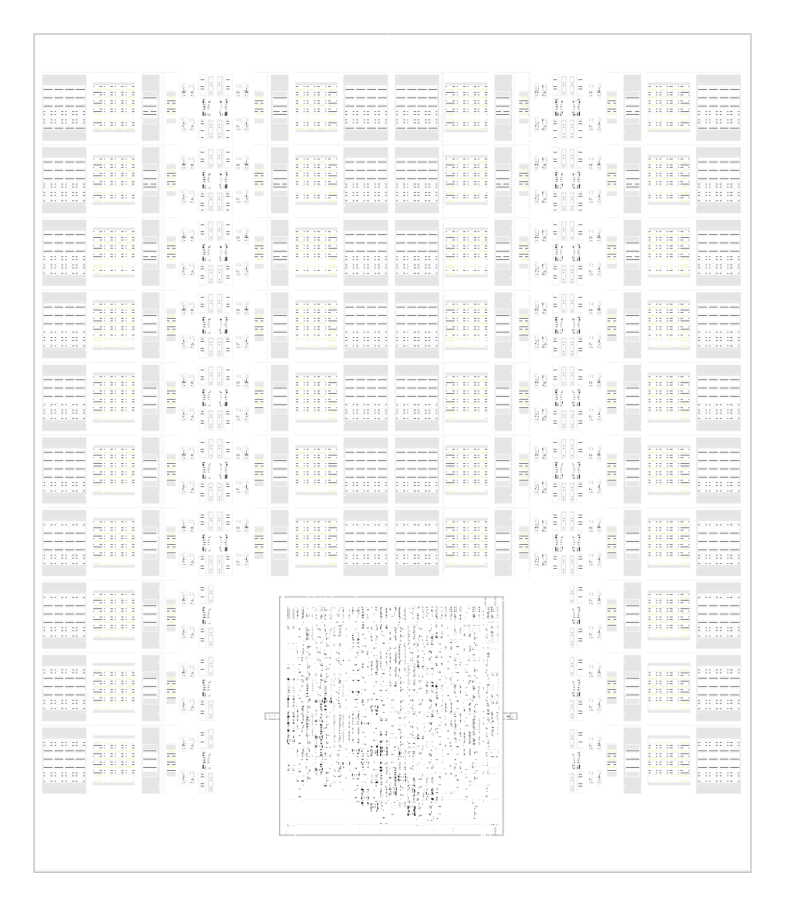
We design the silicon that goes inside our boards — and inside other people's. Configurable digital and analogue blocks, tight DA integration, and a cloud-based design and verification stack. Three months from architecture freeze to tapeout. Six times faster than the status quo.
RISC-V core with hardened cache, FDIR, and bus arbitration. Triplicated state, scrubbed on idle.
22 FDX · 600 MHzLDOs, ADCs, DACs and references. Configurable bias trees; calibrated post-irradiation in firmware.
28 nm bulk · 0.8–3.6 VS-band and X-band transceiver tiles. Direct-conversion, on-die filtering, programmable PA driver.
2.0–8.4 GHz · 2 W TXSynthesis, P&R, and DRC orchestrated in containers. We rebuild the chip overnight; you see the report at 0700.
Constraint-driven placement closes timing on the first pass for ~80% of blocks. The remaining 20% is where engineers earn their keep.
Hardened cells, qualified once, reused across programmes. Each block ships with its own characterisation report and irradiation history.
DA on the same die, with hooks designed in for software-defined behaviour. The system architect and the layout engineer share a Slack channel.
| Mode | What you get | Lead time | NRE |
|---|---|---|---|
| CatalogueStock SPH parts | Hardened blocks, datasheet, eval kit | 8 weeks | — |
| ConfiguredSPH IP, your spec | Re-parameterised block, MPW tapeout | 4 months | € low |
| CustomNew ASIC, full programme | Architecture → tapeout → qualification | 9–12 months | € programme |
Talk to a chip architect, not an account manager.